
The NOT gate, built using an NPN transistor, inverts input signals. The circuit verifies the truth table by showing the LED ON for 0 input and OFF for 1 input.
Apparatus
An NPN transistor (BC547A), two resistors (1–2 kΩ and 20–30 kΩ), a DC power supply (SV), connecting wires, a two-way key, an LED, and a breadboard.
Theory
The NOT gate is a logic gate with one input and one output. It is also known as an inverter because it changes a high input (1) to a low output (0) and vice versa. The Boolean expression for a NOT gate is:
F = Ā
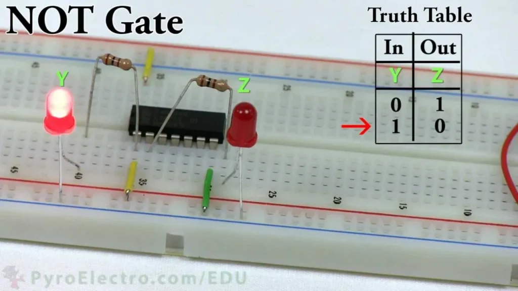
| Input (A) | Output (F = Ā) |
|---|
| Input | Output |
| A | F= |
| 0 | 1 |
| 1 | 0 |
In the basic NOT gate circuit, an NPN transistor is connected in a common-emitter configuration. The output is taken between the collector (C) and emitter (E) terminals, while the base-emitter terminals control the gate operation.
When the input (A = 0), the base current is zero, and the transistor remains in the cut-off region. As a result, no current flows through the collector, and the output is high (1).
However, when the input (A = 1), the base-emitter junction becomes forward-biased. The transistor saturates, allowing maximum current to flow through it. Consequently, the output voltage drops close to 0.2 volts, which represents a low output (0).
Thus, the NOT gate inverts the logic state of the input signal.
Procedure
-
Assemble the circuit on a clean breadboard. Ensure that the resistor RR is approximately twice the value of rr.
-
Ground the input terminal (A = 0). In this condition, the transistor remains in the cut-off region, and no current flows through it. The output voltage becomes maximum (F = 1), and the LED glows. This verifies the first row of the truth table.
-
Next, apply a high voltage to the input terminal (A = 1). A small base current flows through the base-emitter junction, turning the transistor ON. The collector-emitter voltage drops to nearly 0.1 V. As a result, the output becomes 0, and the LED switches OFF. This verifies the second row of the truth table.
Hence, the working of a NOT gate is successfully demonstrated.
Precautions
-
Ensure all connections are neat and tight.
-
Correctly identify the emitter and collector junctions.
-
The base resistor RR should have a large value—about ten times the collector resistance—to limit the base current.
Viva Voce
Q1. Why is the NOT gate known as an inverter?
Ans: Because it reverses the input signal, changing high to low and vice versa.
Q2. What is the combination of an AND gate and a NOT gate called?
Ans: The combination is known as a NAND gate.
Q3. Why does the base resistor RR have a large value?
Ans: The transistor base requires only a small current (in microamperes), so a large resistor limits the current and protects the transistor.
Q4. How does the transistor operate properly?
Ans: It operates correctly when the emitter-base junction is forward-biased, and the collector-base junction is reverse-biased.